Description
SIPLACE CA2 V3: The High-Precision Placement Core of Semiconductor Manufacturing, Defining the Standard for Micron-Level Production
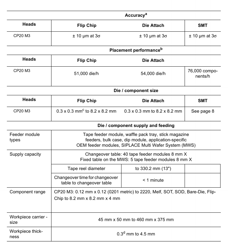
In the micron-level battlefield of semiconductor manufacturing, every breakthrough in precision and efficiency determines the technological advancement. With its ultra-high precision of ±10 μm @ 3σ and full-scenario adaptability, the ASMPT SIPLACE CA2 V3 die placement machine has become a core production tool for semiconductor chip and module packaging, providing stable and reliable manufacturing support for precision processes such as wafer-level packaging, flip chip, and die attach.
Precisely Controlling Semiconductor Placement in All Scenarios
From ultra-micro chips as small as 0.12 mm × 0.12 mm (0201 metric) to large bare dies as large as 8.2 mm × 8.2 mm, the CA2 V3, leveraging the powerful performance of its CP20 M3 placement head, easily handles core semiconductor component types such as bare-die, flip-chip, and SMT. Whether it’s flip chip production at 51,000 dies/h, die attach at 54,000 dies/h, or SMT components at 76,000 components/h, the stable production capacity meets semiconductor mass production demands, further enhancing precision manufacturing efficiency.
Direct wafer supply + intelligent material exchange ensures continuous mass production with zero downtime.
Efficient mass production in semiconductor manufacturing relies on a stable material feeder system. The CA2 V3, equipped with the Multi Wafer System (MWS), directly extracts materials from the wafer. Combined with the Wafer Exchange Unit (WEU), it allows for non-stop wafer exchange, eliminating the downtime and losses associated with traditional material exchange. The SmartFeeder X/Xi supports offline setup and continuous material delivery, with a line change time of less than one minute, making transitions to high-volume, low-volume production of multiple semiconductor products smoother.
Micron-level inspection and full-process traceability strengthen quality assurance.
Semiconductor products have zero tolerance for defects. The CA2 V3’s intelligent vision system provides a comprehensive quality barrier: Cracked Die Detection accurately identifies chip cracks, OnBoard Inspection inspects pads and critical areas in real time, and Pattern Matching technology easily handles the positioning challenges of delicate pads. It also supports barcode reading for various barcodes, including Data Matrix and QR codes. Combined with the WORKS software suite, it enables full data traceability from wafer to finished product, ensuring traceability and control over the production of every chip.
Compliance Certification and Clean Environment Meet the Stringent Requirements of Semiconductor Manufacturing.
Understanding the stringent environmental requirements of semiconductor manufacturing, the CA2 V3 has achieved SEMI S2/S8 safety certification, IEC 61340 ESD anti-static certification, and ISO 14644-1 Cleanroom Class 7 certification. It meets comprehensive standards for equipment safety, ESD protection, and dust control, making it a perfect fit for the demanding production environment of semiconductor cleanrooms.
Choosing the SIPLACE CA2 V3 means choosing the precision benchmark and efficiency engine for semiconductor manufacturing—defining quality with micron-level control and driving mass production with intelligent technology, ensuring that every chip is precisely controllable, efficient, and reliable.SIPSMT